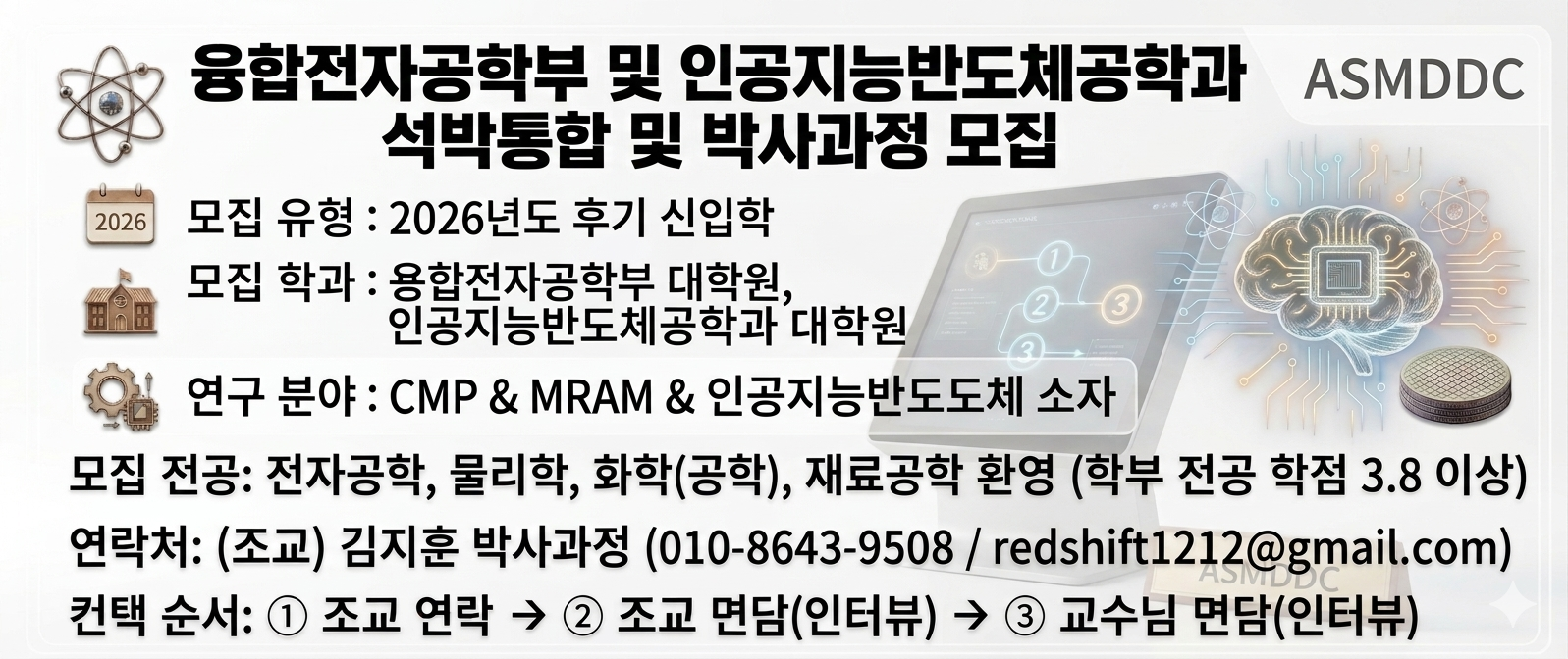
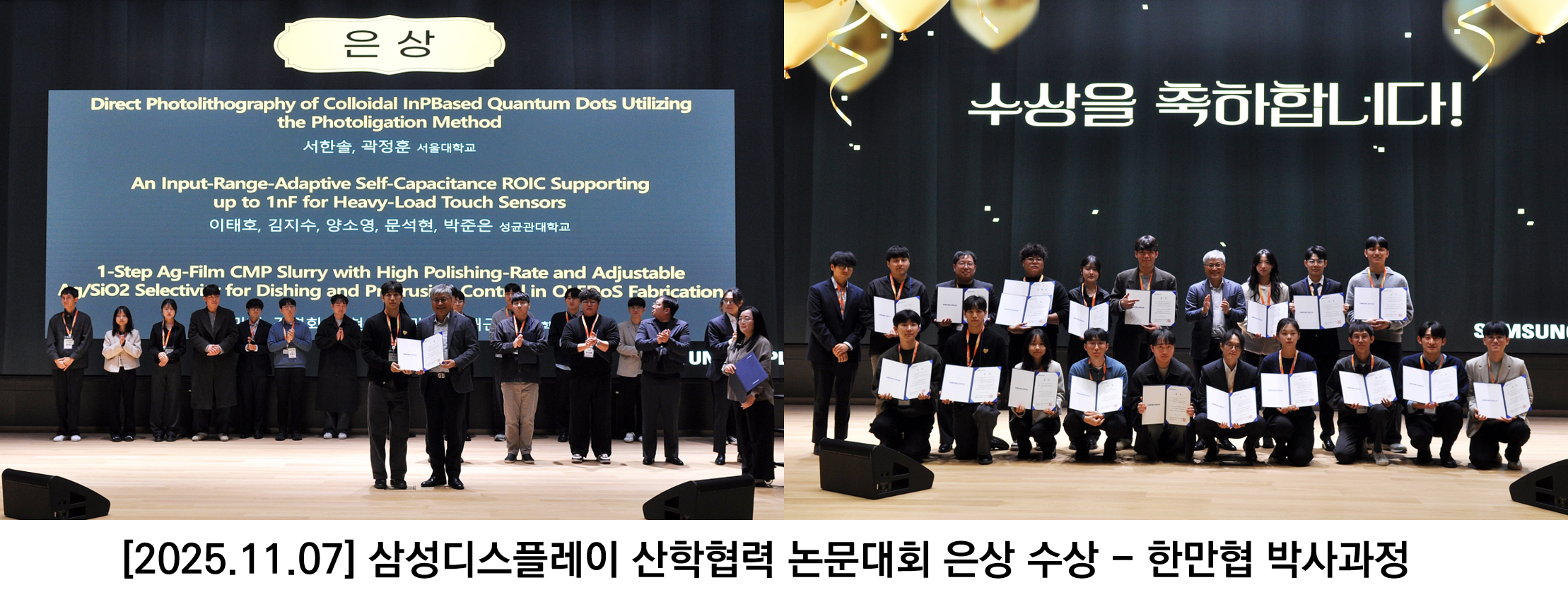
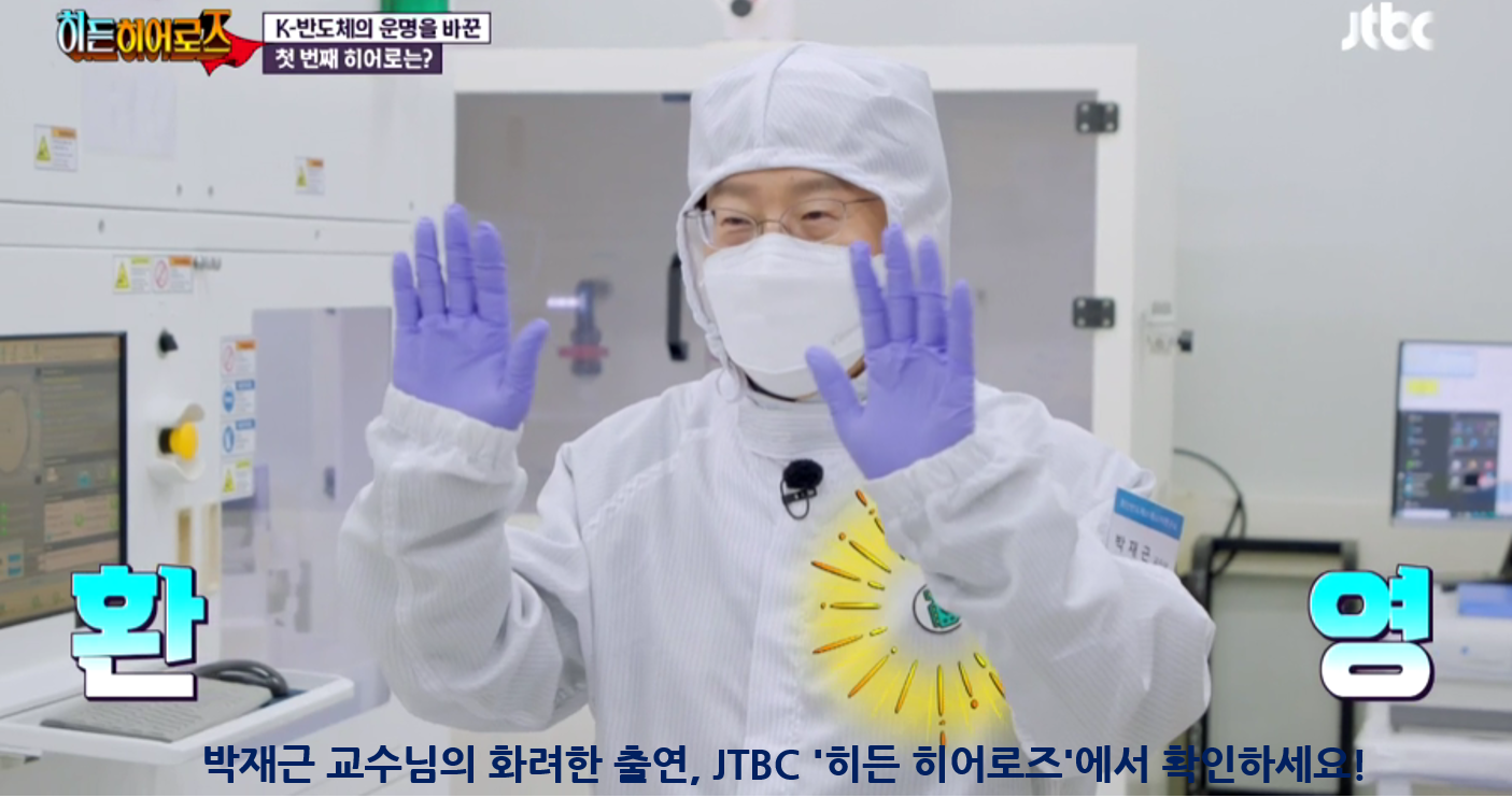
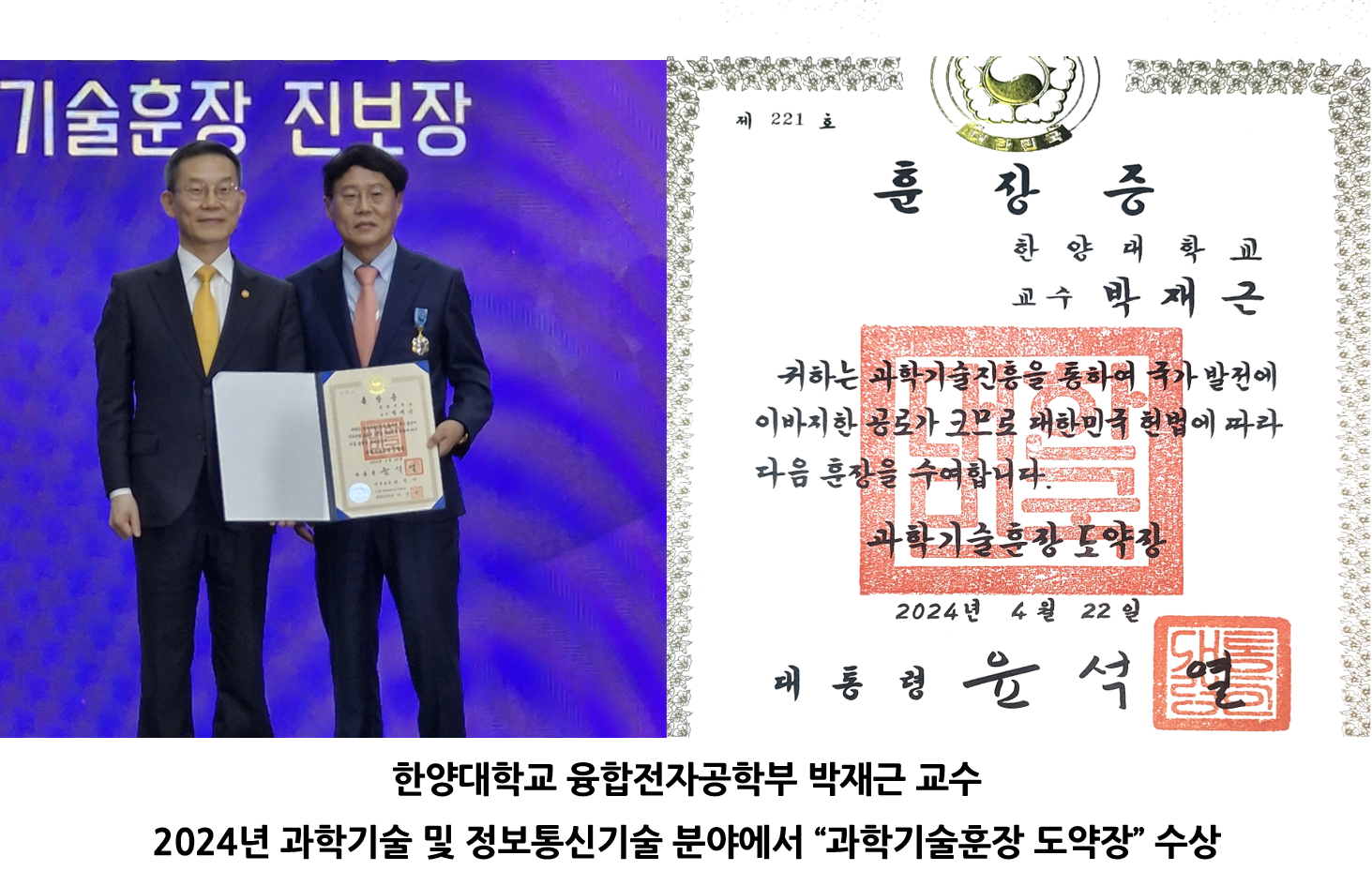
|
350 |
[2021.09.06] Super fine cerium hydroxide abrasives for SiO2 film chemical mechanical planarization performing scratch free
 |
|
349 |
[2021.06.18] Enhanced performance of polymer solar cells using selective silver nanocrystal morphology
|
|
348 |
[2021.06.04] Self-stopping slurry for planarizing extremely high surface film topography in nanoscale semiconductor devices
|
|
347 |
[2021.05.28] Extremely high photoconductivity ultraviolet-light sensor using amorphous In–Ga–Zn–O thin-film-transistor
|
|
346 |
[2021.05.05] Dishing-free chemical mechanical planarization for copper films
|
|
345 |
[2021.04.01] Doping-less tunnel field-effect transistors by compact Si drain frame/Si0.6Ge0.4-channel/Ge source
|
|
344 |
[2021.01.29] Etch characteristics of magnetic tunnel junction materials using H-2/NH3 reactive ion beam
|
|
343 |
[2021.01.13] Design of n+-Base Width of Two-Terminal-Electrode Vertical Thyristor for Cross-Point Memory Cell Without Selector
|
|
342 |
[2020.12.15] Impact of wet ceria abrasive size on initial step height removal efficiency for Isolated SiO2 film chemical mechanical planarization
|
|
341 |
[2020.11.20] Relationship of Free Surface Area with Oxygen Concentration in Silicon Ingot Grown by Czochralski Method for High Efficiency Solar Cells
|
|
340 |
[2020.06.28] An electroforming-free mechanism for Cu2O solid-electrolyte-based conductive-bridge random access memory (CBRAM)
|
|
339 |
[2020.06.22] Influence of Scavenger on Abrasive Stability Enhancement and Chemical and Mechanical Properties for Tungsten-Film Chemical- Mechanical-Planarization
|
|
338 |
[2020.06.18] Multi-level resistance uniformity of double pinned perpendicular magnetic-tunneljunction spin-valve depending on top MgO barrier thickness
|
|
337 |
[2020.06.08] A Bow-free Freestanding GaN Wafer
|
|
336 |
[2020.06.01] Highly Selective Polishing Rate Between a Tungsten Film and a Silicon-Dioxide Film by Using a Malic-Acid Selectivity Agent in Tungsten-Film Chemical-Mechanical Planarization
|