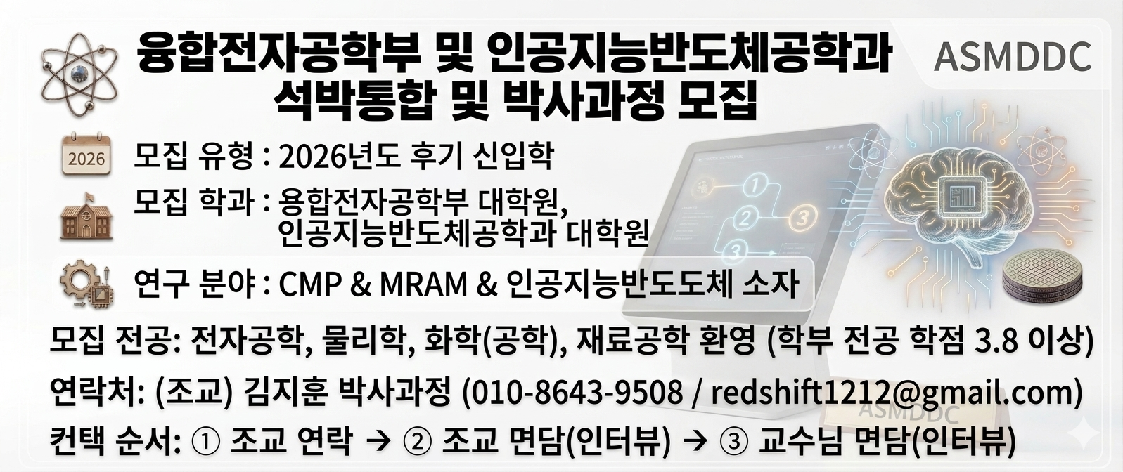
|
20 |
[1997.10.08] Ni/3C-SiC 계면의 Ohmic 특성
 |
|
19 |
[1996.__.__] Effect of Crystal Characteristics on the DRAM Device Yield
|
|
18 |
[1996.__.__] DRAM Wafer Qualification Issues : Oxide integrity vs. D-Defects, Oxygen Precipitates and High Temperature Annealing
|
|
17 |
[1996.11.__] Wafer Engineering for DRAM Devices
|
|
16 |
[1996.11.25] Effect of Crystal Defects on Device Characteristics
|
|
15 |
[1995.__.__] Observation of Structural, Electrical, and Chemical Nature on Multi-ring Wafer
|
|
14 |
[1995.__.__] Nature of D-defect in CZ Silicon : D-defect Dissolution and D-Defect Related T.D.D.B
|
|
13 |
[1995.__.__] Gate Oxide Integrity in DRAM Devices : The Influence of Substrate D-defects
|
|
12 |
[1995.__.__] Effect of H2 Annealing on Oxide Integrity Improvement
|
|
11 |
[1995.__.__] Defect Oxide Defect Detection by Cu-decoration
|
|
10 |
[1995.03.20] Effect of D-defects and Oxygen Precipitates on Oxide Integrity
|
|
9 |
[1994.__.__] Temperature Dependent Electron Beam Induced Current Studies of MOS Capacitor Structures
|
|
8 |
[1994.__.__] Structure and Morphology of "D-defects" in CZ Si
|
|
7 |
[1994.__.__] Correlation of Substrate D-defects in CZ Silicon with MOS Breakdown Site via MOS/EBIC, FIB, and TEM
|
|
6 |
[1994.__.__] Comparison of Oxide Breakdown Mechanisms Due to D-defects and Oxygen Precipitates
|